Program
Students are encouraged to arrive on Monday, March 11, 2013.
Registration will be opened at Kenkyu-honkan from 16:00 to 19:00 on March 11 and at 3-gokan Seminar hall from 8:30 to 9:00 on March 12 .
Tuesday, March 12 and Friday, March 22, will consist of an introduction, necessary training and plenary lectures in the morning, and then Facility Tour to Tsukuba and Tokai campuses in the afternoon.
Wednesday, March 13 through Tuesday, March 21:
Students will start with 90 minutes plenary lecture at 8:30am,
then be split into eight groups, and taken to their respective area.
Students will take two of eight tracks which will
be determined and noticed in advance based on
their preferences on their applications.
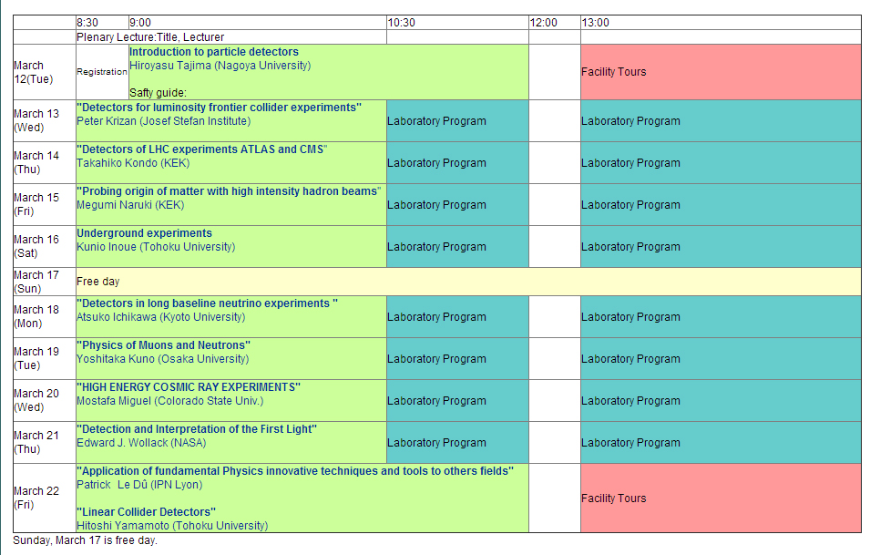
Time Table
link to indico page
There is a special security guard in our indico system in KEK. You'll be asked username and password in a pop-up window when you access our indico site. Please enter username "kds" and the password which is written in the pop-up window. Then, you should be able to access the page. The password will be changed daily.
Laboratory program
Laboratory program will be held in Tsukuba and Tokai Campus.
NEU and TSB programs are in Tokai and the other is in Tsukuba.

| DAQ: FPGA and DAQ system | |
| Convener; Yoichi Igarashi (KEK) Masaharu Nomachi(Osaka Univ.) Shohei Nishida(KEK) 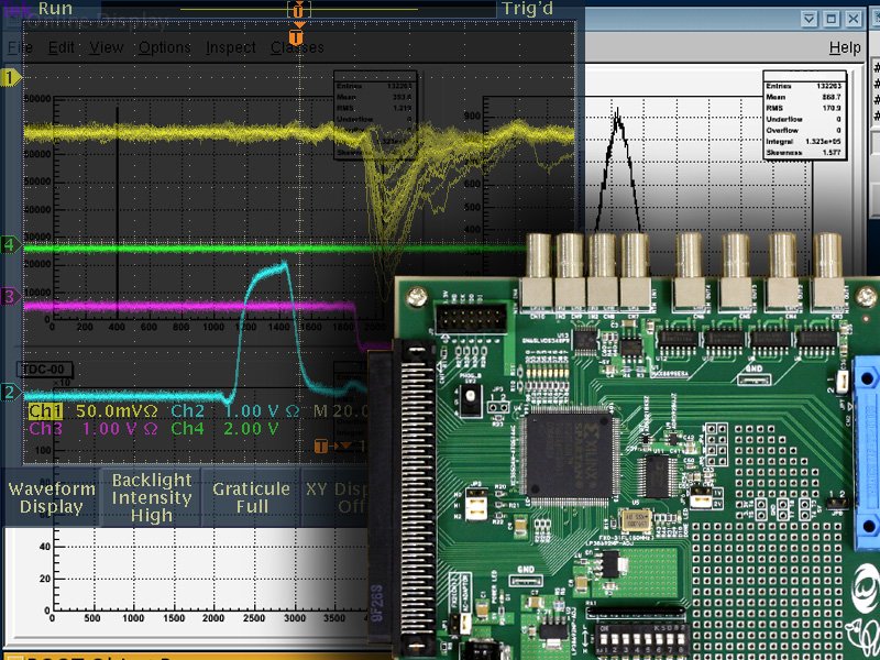 |
The students will have experiences with the mechanism of the digital measurements using FPGA (Field Programmable Gate Array) and the data acquisition (DAQ). |
| STD: Silicon Tracking Detector | |
| Convener; Yoichi Ikegami (KEK) Kazuhiko Hara (Univ. Tsukuba) Tsutomu Mibe(KEK) Ryuma Hori (KEK) Shingo Mitsui (KEK) 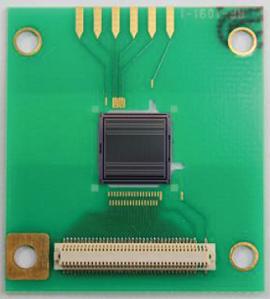 |
Students will start to learn the principle of operation of silicon
sensors, finally they try to reconstruct cosmic ray tracks. |
| NEU: Neutrino Detector | |
| Convener; Masashi Yokoyama (The Univ. of Tokyo) Tsuyoshi Nakaya (Kyoto Univ.) Akihiro Minamino (Kyoto Univ.) Toshifumi Tsukamoto (KEK) Takeshi Nakadaira (KEK) Taku Ishida (KEK) Ken Sakashita(KEK) 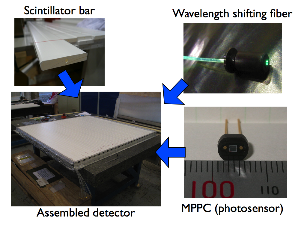
Plastic scintillators, wavelength shifting fibers, MPPCs (photosensors) and an assembled particle (neutrino) detector. |
Neutrino Detector Students will learn the basics of detectors consisting of plastic scintillators, wavelength shifting fibers, and silicon photodetectors (Multi-pixel Photon Counter, MPPC). This type of detector is used as a fundamental block of near neutrino detectors for the T2K accelerator neutrino experiment. They will learn the principle of scintillator, light collection using wavelength shifting fibers, and operation of MPPC through measurements of their properties. In the end, they will construct a small detector using the above technique, detect real partilces (e.g. from neutrino beam, charged particle beam, or cosmic ray), and evaluate the performance of constructed detector as an integrated particle detection system. |
| SUP: Superconducting Detector | |
| Convener; Atsuko Kibayashi (Okayama Univ.) Jihoon Choi (Korea Univ.) Mitsuhiro Yoshida (KEK) Masashi Hazumi (KEK) Nobuaki Sato (KEK) Hirokazu Ishino (Okayama Univ.) 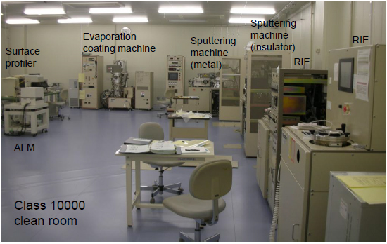 Class 10k cleanroom facility at KEK |
Microwave Kinetic Inductance Detectors (MKIDs) are a kind of superconducting detectors. Since the MKIDs were first devised a decade ago, they have gained much attention for their simple approach to multiplexing and making large arrays. They are especially recognized as next-generation detectors in millimeter and sub-millimeter astronomy including measurements of the Cosmic Microwave Background, and also as phonon detectors in the dark matter search. In the Class 100k cleanroom, students will learn how to operate the dicing saw to cut the wafer to make individual chips, and use the wire bonder to integrate the chip with readout electronics. Finally students will place the chip in the Helium-3 sorption refrigerator to cool it down 0.3K, measure the resonance peaks with a vector network analyzer and power of the injected millimeter wave, and evaluate their own MKIDs’ performance. |
| PHD: Photon Detector | |
| Convener; Koji Yoshimura (KEK) Ichiro Adachi (KEK) Isamu Nakamura (KEK) Peter Krizan (Ljubljana Univ.) Samo Korpar (Ljubljana Univ.) 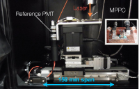 
|
The objective of this course is to learn the basics of two typical photon sensors, photo-multiplier tube (PMT) and Geiger-mode APD (SiPM/MPPC), both of which are now commonly used in various experiments. Starting with learning how to operate sensors, calibration and evaluation of the various characteristics are performed through comparison of the sensors. These basics would be essential to design and operate the particle detectors with various types of photon sensors. The practical course is organized as following subjects and learnings.
Making the hardware for testing the devices, i.e. circuit boards to apply bias voltage to SiPM/MPPC and to drive LED, and simple dark box for light-shield.
Readout electronics (NIM, CAMAC), simple data acquisition system, and data analysis (some statistics)
Temperature dependences of each characteristics.
Photon detection efficiency with different wavelength light. |
| LIQ: Liquid Noble Gas Detector | |
| Convener; Toshiaki Tauchi (KEK) Takasumi Maruyama (KEK) Satoshi Mihara (KEK) Katsuyu Kasami (KEK) Akihiro Maki (KEK) Takayuki Saeki (KEK) Shuji Tanaka (KEK) Tomiyoshi Haruyama (KEK) Shogo Nakamura (Yokohama National Univ.) Toshinori Mori(Univ. of Tokyo) Akira Sugiyama (Saga Univ.) Masayuki Kumada (NIRS) 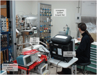 Experimental setup for test of prototype TPC with liquid xenon. The cryogenic system consists of a control panel, cryogenic cooler of pulse tube type, compressor, vacuum pumps, a purification getter and a storage tank of xenon gas. The data acquisition system consists of NIM and CAMAC modules. Also, the data can be analyzed by using digital oscilloscopes. |
Students will learn basic properties of liquid noble gas detector by observing scintillation lights and ionization charges. They also learn how gamma rays interact with the noble gas characterizing photoelectric effect, Compton scattering by using various radiation sources. Since alpha particles and neutrons interact differently from gammas and electrons with the noble gas, the particle species can be discriminated by time envelop of scintillation lights. The ionization charges will be detected in a Time Projection Chamber (TPC), where three dimensional position of interaction is measured as well as amount of charges. Students will learn the principle of TPC. Especially, students will discuss a mechanism of charge transfer through a measurement of charge drift velocity in TPC. Correlation between scintillation lights and ionization charges is an interesting subject for dark matter searches. Noble gases are liquefied at low temperature, i.e. 87K and 165K for argon and xenon, respectively, at 1 atmosphere. Students will learn a principle of cryogenic system with purification at impurity of ppb (parts per billion) level. There will be lectures on experiments (ICARUS, MEG, XMASS, XENON etc.) and medical application (PET) with the use of liquid noble gas detector. |
| GAS: Gas Tracking Detector | |
| Convener; Shoji Uno (KEK) Kyoichiro Ozawa(KEK) Kentaro Miuchi(Kobe Univ.) 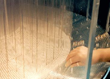 Photograph of Cylindrical Drift Chamber, which is commonly used at particle physics experiments |
Objects of the course is to know basics of gas tracking detectors thorough
several hands-on experiences. Students will learn about several features of
the interactions between particles and materials.
|
| TSB: Practice with Test Beam | |
Convener; Kyoichiro Ozawa (KEK)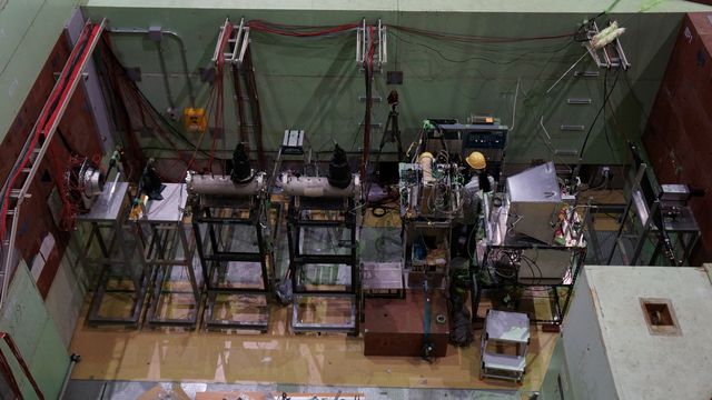 Photograph of K1.1 BR experimental area at J-PARC hadron hall with some
detectors. Photograph of K1.1 BR experimental area at J-PARC hadron hall with some
detectors. |
This course aims to provide experiences about a detector test using a beam.
The course will be carried out at Hadron-hall in J-PARC, Tokai. Students
will learn about basic handlings of tracking and particle identification
detectors. |